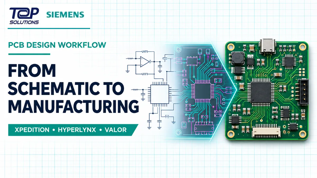
A PCB can pass connectivity checks and still fail on signal behavior, power delivery or manufacturability. This workflow assigns each review to the right stage: Xpedition for design, HyperLynx for signal and power analysis, and Valor for DFM.
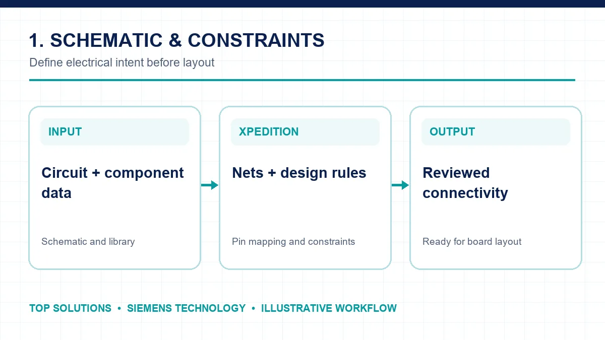
1. From schematic to layout inputs
Before placement, review the schematic, libraries, pin mapping, netlist and critical constraints. These may include trace length, differential pairs, reference planes and clearances. Xpedition carries electrical intent into rule-driven PCB design. The handoff is a reviewed connectivity model and a usable constraint set, not just a schematic drawing.
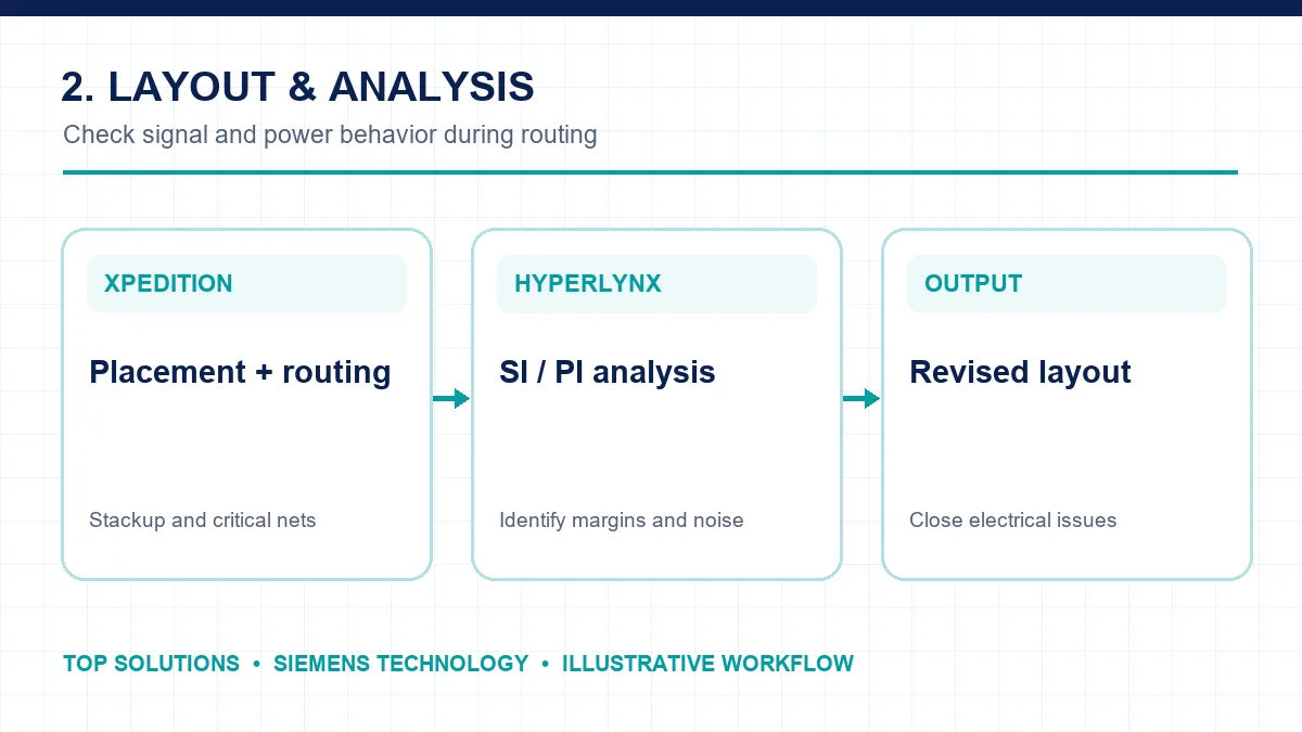
2. Layout with signal and power checks
During placement and routing, define the stackup, connector locations, return paths and sensitive nets. HyperLynx supports signal integrity (SI) and power integrity (PI) analysis to check reflections, crosstalk, voltage drop and power behavior against design margins. Findings can drive trace, plane or decoupling changes before the layout is frozen.
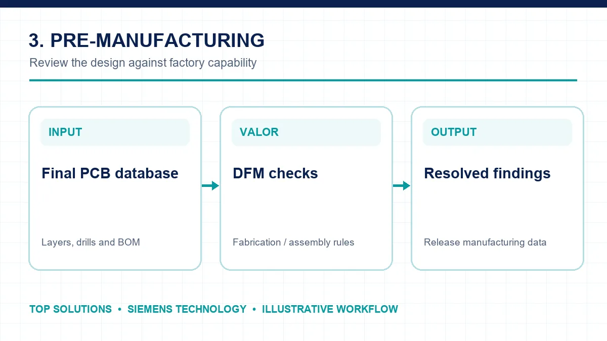
3. DFM before manufacturing release
Electrical DRC does not cover every fabrication or assembly constraint. Valor compares the near-final design with factory rules such as copper spacing, drills, solder mask and component assembly clearances. Each finding should be resolved or consciously accepted with a reason. Only then should the team release manufacturing data and the aligned BOM.
Handoffs at a glance
| Stage | Input | Output |
|---|---|---|
| Xpedition | Schematic, libraries, constraints | PCB layout and design database |
| HyperLynx | Stackup, critical nets, layout | SI/PI findings and design changes |
| Valor | Near-final design and factory rules | Resolved DFM report |
The depth of analysis depends on signal speed, reliability targets and the selected manufacturer’s capability. A simple board and a dense high-speed board require different review effort.
Technical source: Siemens EDA – PCB products.